Browse Course Material
Course info, instructors.
- Prof. David Cory
- Prof. Ian Hutchinson
- Prof. Manos Chaniotakis

Departments
- Electrical Engineering and Computer Science
- Nuclear Science and Engineering
As Taught In
- Electronics
- Signal Processing
- Differential Equations
Learning Resource Types
Introduction to electronics, signals, and measurement, 17_diodes1.pdf.
This resource contains information on diodes, ideal diode model, full diode model, offset voltage model, half wave rectifier, full awve rectifier, and zener diode.

You are leaving MIT OpenCourseWare
Zener Diode Basics (A Beginner’s Guide)
In this guide, you’ll learn exactly how a Zener diode works and how to use it in circuits.
Did you know that some of the common things you can build with Zener diodes include simple power supplies and guitar pedals?
Sounds interesting? Let’s jump in!

What Is a Zener Diode?
A Zener diode is a type of diode that is often used for voltage regulators and shaping waveforms.
Its symbol is an arrow pointing towards a crooked line. There are actually three different ways you can draw the Zener diode symbol in schematics :

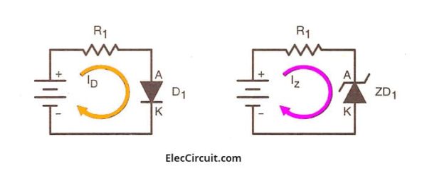
While a normal diode only allows current to flow through a circuit when it is forward-biased (current going from anode to cathode), the Zener diode also works when it is reverse-biased (current going in the opposite direction).
With standard diodes, if you place it in reverse, no current flows.
At least, so it appears. But actually, if you apply enough voltage in reverse, current will start to flow.

10 Simple Steps to Learn Electronics
Electronics is easy when you know what to focus on and what to ignore. Learn what "the basics" really is and how to learn it fast.
This voltage is called the breakdown voltage of the diode.
For example, the rectifier diode 1N4001 has a breakdown voltage of 50V.
The Zener diode is basically the same as the standard PN junction diode. However, it is specially designed to work in reverse bias with a low and specified reverse breakdown voltage.

So, why is that interesting?
Because you’re not limited to the standard forward voltage of 0.7V. You can design the breakdown voltage to be for example 3.3V or 12V – or many other voltages. The manufacturers call this Zener Voltage (Vz) .
This means a Zener diode can act as a voltage regulator because it keeps the breakdown voltage at a nearly constant value across its terminals.
How To Make A Zener Diode Voltage Regulator
Making a voltage regulator is easy with the Zener: Just add a resistor!

Here’s how it works:
When a voltage (must be higher than the Zener voltage) is applied across the resistor and Zener diode, the diode starts conducting in reverse and keeps the voltage drop across it at a constant value of 3.3V.
The rest of the voltage drops across the resistor. This means the resistor acts as a current-limiting resistor so that you can easily calculate the current by using Ohm’s law .

The resistor (R S ) limits the maximum current that can flow through the circuit. If there is no load connected to the circuit all the current flows through the Zener diode, causing it to dissipate its maximum power.
A smaller value of resistor R S gives you a higher maximum current. But at the same time, you have to make sure that you don’t exceed the maximum power rating of the Zener. Therefore, it’s important to choose the right value of series resistance.
Example: Choosing a resistor for a 12V to 3.3V voltage regulator
In this example, you’re going to use a Zener diode that can handle up to 2W of power. What’s a suitable value for the resistor (R S )?

First, you need to find the maximum current that can flow through the Zener diode:

That means that the minimum value of the resistor is:

So a value of 14.5 Ω is the absolute minimum. But you can use higher resistances of course.
Next, you need to check how much current your load needs. The load resistor is 1 kΩ, so its current is calculated as follows:

That’s much lower than the 0.6A you’d get from the 14.5 Ω resistor, so no problem here.
If you want to use a higher resistor value, just use the following formula with your chosen resistor value and make sure that it’s above the current you need for your load:

For example, if you want to use a 100 Ω resistor, this would give you a maximum current of:

Still, high above the needed 0.0033A for the load, so you’re good to go.
That said, Zener diodes have their disadvantages. Check out this article about why Zener diodes make lousy voltage generators .
Wave-Shaping With the Zener
In the previous example, you saw how the Zener works with DC power. However, what happens when it’s used with AC power? How would it react to a constantly changing signal such as an audio signal?
Check out the following circuit:

In the above diagram, the Zener diode has a V Z of 5V, so if the waveform exceeds this limit, the diode will “clip off” the excess voltage from the input, resulting in a waveform with a flat top maintaining a constant output of 5V.
When forward-biased, the Zener diode behaves like a regular diode. So when the waveform reaches negative values below 0.7V, the Zener acts like a typical rectifier diode, resulting in output clipping at -0.7V.
Zener Diode Example: Distortion Guitar Pedal
Diode clipping and clamping circuits can shape a waveform to produce an output waveform with a different shape. A clipper circuit clips off the positive or negative part of an AC signal, which is why they are commonly used as waveform shaping circuits.

When you cut off the top of an audio signal, it sounds distorted. This is exactly what you want in a distortion guitar pedal!
But the output signal of an electric guitar isn’t high enough to be clipped. So in order to clip it, you must amplify it first. Here’s a basic guitar distortion pedal circuit that uses Zener diodes to distort the sound:
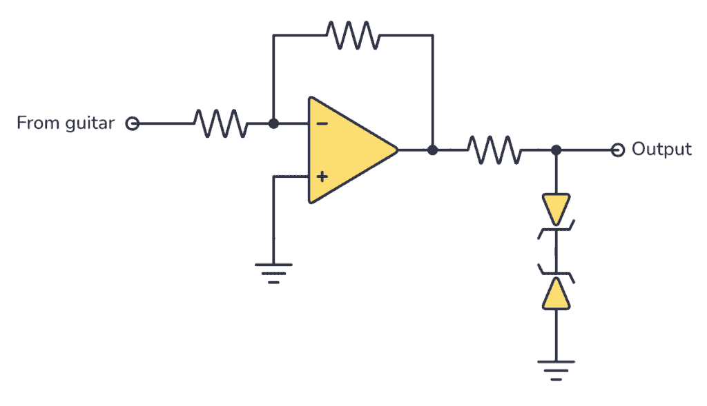
So, if you build the circuit above the output waveform will be clipped at the V Z voltage plus 0.7V, which is the forward voltage drop of the other diode.
Zener Diode Characteristics (The I-V Graph)

The I-V characteristics curve of a Zener diode is shown in the image above. By studying this graph, it becomes clear why Zener diodes are employed in reverse bias.
By observing the behavior of a Zener diode, you can notice that as the reverse voltage rises, the reverse current also increases gradually until it hits the Zener knee current, I Z (min). At this point, the breakdown effect starts, and the Zener impedance (Z Z ), which is the internal resistance of the diode, begins to rapidly decrease as the reverse current increases.
In general, the breakdown voltage of the Zener (V Z ) is fairly constant, although it increases slightly with increasing Zener current (I Z ). V Z is commonly set at a value of the Zener current known as the I Z (min).
A Zener diode’s ability to maintain almost constant voltage in its breakdown region makes it suitable for regulating voltage even in the simplest voltage regulator applications.
A voltage regulator’s main role is to deliver a steady output voltage to a load connected in parallel. This is even when the supply voltage has ripples or the load current varies. Zener diodes can maintain a constant voltage output as long as their reverse breakdown region holding current does not drop below I Z (min).
Common Zener Diode Voltages
Here you have a table with the most common Zener voltages in diodes of 0.3 W and 1.3 W.
| 2.4V | 2.7V | 3.0V | 3.3V | 3.6V | 3.9V | 4.3V | 4.7V |
| 5.1V | 5.6V | 6.2V | 6.8V | 7.5V | 8.2V | 9.1V | 10V |
| 11V | 12V | 13V | 15V | 16V | 18V | 20V | 22V |
| 24V | 27V | 30V | 33V | 36V | 39V | 43V | 47V |
| .3V | 3.6V | 3.9V | 4.3V | 4.7V | 5.1V | 5.6 | 6.2V |
| 6.8V | 7.5V | 8.2V | 9.1V | 10V | 11V | 12V | 13V |
| 15V | 16V | 18V | 20V | 22V | 24V | 27V | 30V |
| 33V | 36V | 39V | 43V | 47V | 51V | 56V | 62V |
More Diodes Tutorials
- What is a Diode?
- Types of Diodes
- The Light-Emitting Diode (LED)
- Laser Diodes
- Photodiodes
- Rectifier Diodes
- Zener Diodes
- Schottky Diodes
- Diode Bridge Rectifier

Get Our Basic Electronic Components Guide
Learn how the basic electronic components work so that circuit diagrams will start making sense to you.
- Network Sites:
- Technical Articles
- Market Insights

- Or sign in with
- iHeartRadio
- What Are Zener Diodes?
Join our Engineering Community! Sign-in with:
- Semiconductors
Diodes and Rectifiers
- Introduction to Diodes And Rectifiers
- Meter Check of a Diode
- Diode Ratings
- Rectifier Circuits
- Peak Detector
- Clipper Circuits
- Clamper Circuits
- Voltage Multipliers (Doublers, Triplers, Quadruplers, and More)
- Inductor Commutating Circuits
- Diode Switching Circuits
- Special-purpose Diodes
- Other Diode Technologies
- SPICE Models
What Is a Zener Diode?
A Zener diode is a special type of rectifying diode that can handle breakdown due to reverse breakdown voltage without failing completely. Here we will discuss the concept of using diodes to regulate voltage drop and how the Zener diode operates in reverse-bias mode to regulate voltage in a circuit.
How Diodes Regulate Voltage Drop
If we connect a diode and resistor in series with a DC voltage source so that the diode is forward-biased, the voltage drop across the diode will remain fairly constant over a wide range of power supply voltages as in figure(a) below .
The current through a forward-biased PN junction is proportional to e raised to the power of the forward voltage drop. Because this is an exponential function, current rises quite rapidly for modest increases in voltage drop.
Another way of considering this is to say that voltage dropped across a forward-biased diode changes little for large variations in diode current. In the circuit shown in figure (a) below, diode current is limited by the voltage of the power supply, the series resistor, and the diode’s voltage drop, which as we know doesn’t vary much from 0.7 volts.

Forward biased Si reference: (a) single diode, 0.7V, (b) 10-diodes in series 7.0V.
If the power supply voltage were to be increased, the resistor’s voltage drop would increase almost the same amount, and the diode’s voltage would drop just a little. Conversely, a decrease in power supply voltage would result in an almost equal decrease in resistor voltage drop, with just a little decrease in diode voltage drop.
In a word, we could summarize this behavior by saying that the diode is regulating the voltage drop at approximately 0.7 volts.
The Use of Voltage Regulation
Voltage regulation is a useful diode property to exploit. Suppose we were building some kind of circuit which could not tolerate variations in power supply voltage, but needed to be powered by a chemical battery, whose voltage changes over its lifetime. We could form a circuit as shown above and connect the circuit requiring steady voltage across the diode, where it would receive an unchanging 0.7 volts.
This would certainly work, but most practical circuits of any kind require a power supply voltage in excess of 0.7 volts to properly function. One way we could increase our voltage regulation point would be to connect multiple diodes in series so that their individual forward voltage drops of 0.7 volts each would add to create a larger total.
For instance, in our example above [figure(b)], if we had ten diodes in series, the regulated voltage would be ten times 0.7, or 7 volts.
So long as the battery voltage never sagged below 7 volts, there would always be about 7 volts dropped across the ten-diode “stack.”
How Zener Diodes Regulate Voltage
If larger regulated voltages are required, we could either use more diodes in series (an inelegant option, in my opinion) or try a fundamentally different approach.
We know that diode forward voltage is a fairly constant figure under a wide range of conditions, but so is reverse breakdown voltage. Breakdown voltage is typically much, much greater than forward voltage.
If we reversed the polarity of the diode in our single-diode regulator circuit and increased the power supply voltage to the point where the diode “broke down” (that is, it could no longer withstand the reverse-bias voltage impressed across it), the diode would similarly regulate the voltage at that breakdown point, not allowing it to increase further. This is shown in figure(a) below.

(a) Reverse biased Si small-signal diode breaks down at about 100V. (b) Symbol for Zener diode.
Unfortunately, when normal rectifying diodes “break down,” they usually do so destructively. However, it is possible to build a special type of diode that can handle breakdown without failing completely. This type of diode is called a Zener diode , and its symbol is shown in the figure(b) above .
When forward-biased, Zener diodes behave much the same as standard rectifying diodes: they have a forward voltage drop which follows the “diode equation” and is about 0.7 volts. In reverse-bias mode, they do not conduct until the applied voltage reaches or exceeds the so-called Zener voltage , at which point the diode is able to conduct substantial current, and in doing so will try to limit the voltage dropped across it to that Zener voltage point.
So long as the power dissipated by this reverse current does not exceed the diode’s thermal limits, the diode will not be harmed. For this reason, Zener diodes are sometimes referred to as “breakdown diodes.”
Zener Diode Circuit
Zener diodes are manufactured with Zener voltages ranging anywhere from a few volts to hundreds of volts. This Zener voltage changes slightly with temperature, and like common carbon-composition resistor values, may be anywhere from 5 percent to 10 percent in error from the manufacturer’s specifications. However, this stability and accuracy is generally good enough for the Zener diode to be used as a voltage regulator device in common power supply circuit in the figure below.

Zener diode regulator circuit, Zener voltage = 12.6V).
Zener Diode Operation Please take note of the Zener diode’s orientation in the above circuit: the diode is reverse-biased , and intentionally so. If we had oriented the diode in the “normal” way, so as to be forward-biased, it would only drop 0.7 volts, just like a regular rectifying diode. If we want to exploit this diode’s reverse breakdown properties, we must operate it in its reverse-bias mode. So long as the power supply voltage remains above the Zener voltage (12.6 volts, in this example), the voltage dropped across the Zener diode will remain at approximately 12.6 volts.
Like any semiconductor device, the zener diode is sensitive to temperature. Excessive temperature will destroy a zener diode, and because it both drops voltage and conducts current, it produces its own heat in accordance with Joule’s Law (P=IE). Therefore, one must be careful to design the regulator circuit in such a way that the diode’s power dissipation rating is not exceeded. Interestingly enough, when Zener diodes fail due to excessive power dissipation, they usually fail shorted rather than open. A diode failed in this manner is readily detected: it drops almost zero voltage when biased either way, like a piece of wire.
Mathematical Analysis of Zener Diode Regulating Circuit
Let’s examine a Zener diode regulating circuit mathematically, determining all voltages, currents, and power dissipations. Taking the same form of circuit shown earlier, we’ll perform calculations assuming a Zener voltage of 12.6 volts, a power supply voltage of 45 volts, and a series resistor value of 1000 Ω (we’ll regard the Zener voltage to be exactly 12.6 volts so as to avoid having to qualify all figures as “approximate” in Figure(a) below
If the Zener diode’s voltage is 12.6 volts and the power supply’s voltage is 45 volts, there will be 32.4 volts dropped across the resistor (45 volts - 12.6 volts = 32.4 volts). 32.4 volts dropped across 1000 Ω gives 32.4 mA of current in the circuit. (Figure below (b))

(a) Zener Voltage regulator with 1000 Ω resistor. (b) Calculation of voltage drops and current.
Power is calculated by multiplying current by voltage (P=IE), so we can calculate power dissipations for both the resistor and the Zener diode quite easily:

A Zener diode with a power rating of 0.5 watts would be adequate, as would a resistor rated for 1.5 or 2 watts of dissipation.
Zener Diode Circuit with Higher Resistances
If excessive power dissipation is detrimental, then why not design the circuit for the least amount of dissipation possible? Why not just size the resistor for a very high value of resistance, thus severely limiting current and keeping power dissipation figures very low? Take this circuit, for example, with a 100 kΩ resistor instead of a 1 kΩ resistor. Note that both the power supply voltage and the diode’s Zener voltage in the figure below are identical to the last example:

Zener regulator with 100 kΩ resistor.
With only 1/100 of the current we had before (324 µA instead of 32.4 mA), both power dissipation figures should be 100 times smaller:

Considerations with Load Resistance
Seems ideal, doesn’t it? Less power dissipation means lower operating temperatures for both the diode and the resistor, and also less wasted energy in the system, right? A higher resistance value does reduce power dissipation levels in the circuit, but it unfortunately introduces another problem. Remember that the purpose of a regulator circuit is to provide a stable voltage for another circuit . In other words, we’re eventually going to power something with 12.6 volts, and this something will have a current draw of its own.
Lower value Dropping Resistor Consideration
Consider our first regulator circuit, this time with a 500 Ω load connected in parallel with the Zener diode in the figure below.

Zener regulator with 1000 Ω series resistor and 500 Ω load.
If 12.6 volts is maintained across a 500 Ω load, the load will draw 25.2 mA of current. In order for the 1 kΩ series “dropping” resistor to drop 32.4 volts (reducing the power supply’s voltage of 45 volts down to 12.6 across the Zener), it still must conduct 32.4 mA of current. This leaves 7.2 mA of current through the Zener diode.
Higher value dropping Resistor Consideration
Now consider our “power-saving” regulator circuit with the 100 kΩ dropping resistor, delivering power to the same 500 Ω load. What it is supposed to do is maintain 12.6 volts across the load, just like the last circuit. However, as we will see, it cannot accomplish this task. (Figure below)

Zener non-regulator with 100 KΩ series resistor with 500 Ω load.>
With the larger value of dropping resistor in place, there will only be about 224 mV of voltage across the 500 Ω load, far less than the expected value of 12.6 volts! Why is this? If we actually had 12.6 volts across the load, it would draw 25.2 mA of current, as before. This load current would have to go through the series dropping resistor as it did before, but with a new (much larger!) dropping resistor in place, the voltage dropped across that resistor with 25.2 mA of current going through it would be 2,520 volts! Since we obviously don’t have that much voltage supplied by the battery, this cannot happen.
Higher Dropping resistance Analysis Without Zener Diode
The situation is easier to comprehend if we temporarily remove the Zener diode from the circuit and analyze the behavior of the two resistors alone in the figure below.

Non-regulator with Zener removed.
Both the 100 kΩ dropping resistor and the 500 Ω load resistance are in series with each other, giving a total circuit resistance of 100.5 kΩ. With a total voltage of 45 volts and a total resistance of 100.5 kΩ, Ohm’s Law (I=E/R) tells us that the current will be 447.76 µA. Figuring voltage drops across both resistors ( E=IR ), we arrive at 44.776 volts and 224 mV, respectively.
If we were to re-install the Zener diode at this point, it would “see” 224 mV across it as well, being in parallel with the load resistance. This is far below the Zener breakdown voltage of the diode and so it will not “break down” and conduct current. For that matter, at this low voltage the diode wouldn’t conduct even if it were forward-biased! Thus, the diode ceases to regulate voltage. At least 12.6 volts must be dropped across to “activate” it.
The analytical technique of removing a Zener diode from a circuit and seeing whether or not enough voltage is present to make it conduct is a sound one. Just because a Zener diode happens to be connected in a circuit doesn’t guarantee that the full Zener voltage will always be dropped across it! Remember that Zener diodes work by limiting voltage to some maximum level; they cannot make up for a lack of voltage.
Rule in Zener Diode Regulation Operation
In summary, any Zener diode regulating circuit will function so long as the load’s resistance is equal to or greater than some minimum value. If the load resistance is too low, it will draw too much current, dropping too much voltage across the series dropping resistor, leaving insufficient voltage across the Zener diode to make it conduct. When the Zener diode stops conducting current, it can no longer regulate voltage, and the load voltage will fall below the regulation point.
Calculating Load Resistance for Certain Dropping Resistors
Our regulator circuit with the 100 kΩ dropping resistor must be good for some value of load resistance, though. To find this acceptable load resistance value, we can use a table to calculate resistance in the two-resistor series circuit (no diode), inserting the known values of total voltage and dropping resistor resistance, and calculating for an expected load voltage of 12.6 volts:

With 45 volts of total voltage and 12.6 volts across the load, we should have 32.4 volts across R dropping :

With 32.4 volts across the dropping resistor, and 100 kΩ worth of resistance in it, the current through it will be 324 µA:

Being a series circuit, the current is equal through all components at any given time:

Calculating load resistance is now a simple matter of Ohm’s Law (R = E/I), giving us 38.889 kΩ:

Thus, if the load resistance is exactly 38.889 kΩ, there will be 12.6 volts across it, diode or no diode. Any load resistance smaller than 38.889 kΩ will result in a load voltage less than 12.6 volts, diode or no diode. With the diode in place, the load voltage will be regulated to a maximum of 12.6 volts for any load resistance greater than 38.889 kΩ.
With the original value of 1 kΩ for the dropping resistor, our regulator circuit was able to adequately regulate voltage even for a load resistance as low as 500 Ω. What we see is a tradeoff between power dissipation and acceptable load resistance. The higher-value dropping resistor gave us less power dissipation, at the expense of raising the acceptable minimum load resistance value. If we wish to regulate voltage for low-value load resistances, the circuit must be prepared to handle higher power dissipation.
How Zener Diode do Voltage Regulation
Zener diodes regulate voltage by acting as complementary loads, drawing more or less current as necessary to ensure a constant voltage drop across the load. This is analogous to regulating the speed of an automobile by braking rather than by varying the throttle position: not only is it wasteful, but the brakes must be built to handle all the engine’s power when the driving conditions don’t demand it.
Despite this fundamental inefficiency of design, Zener diode regulator circuits are widely employed due to their sheer simplicity. In high-power applications where the inefficiencies would be unacceptable, other voltage-regulating techniques are applied. But even then, small Zener-based circuits are often used to provide a “reference” voltage to drive a more efficient amplifier circuit controlling the main power.
Common Zener Diode Voltages
Zener diodes are manufactured in standard voltage ratings listed in Table below. The table “Common Zener diode voltages” lists common voltages for 0.3W and 1.3W parts. The wattage corresponds to die and package size and is the power that the diode may dissipate without damage.
Common Zener diode voltages
| 0.5W | ||||||
| 2.7V | 3.0V | 3.3V | 3.6V | 3.9V | 4.3V | 4.7V |
| 5.1V | 5.6V | 6.2V | 6.8V | 7.5V | 8.2V | 9.1V |
| 10V | 11V | 12V | 13V | 15V | 16V | 18V |
| 20V | 24V | 27V | 30V | |||
| 1.3W | ||||||
| 4.7V | 5.1V | 5.6V | 6.2V | 6.8V | 7.5V | 8.2V |
| 9.1V | 10V | 11V | 12V | 13V | 15V | 16V |
| 18V | 20V | 22V | 24V | 27V | 30V | 33V |
| 36V | 39V | 43V | 47V | 51V | 56V | 62V |
| 68V | 75V | 100V | 200V |
Zener diode clipper: A clipping circuit which clips the peaks of waveform at approximately the Zener voltage of the diodes. The circuit of Figure below has two Zeners connected series opposing to symmetrically clip a waveform at nearly the Zener voltage. The resistor limits current drawn by the Zeners to a safe value.
|
|
Zener diode clipper:
The Zener breakdown voltage for the diodes is set at 10 V by the diode model parameter “bv=10” in the spice net list in Figure above. This causes the Zeners to clip at about 10 V. The back-to-back diodes clip both peaks. For a positive half-cycle, the top Zener is reverse biased, breaking down at the Zener voltage of 10 V. The lower Zener drops approximately 0.7 V since it is forward biased. Thus, a more accurate clipping level is 10+0.7=10.7V. Similar negative half-cycle clipping occurs a -10.7 V. (Figure below) shows the clipping level at a little over ±10 V.

Zener diode clipper: v(1) input is clipped at waveform v(2).
- Zener diodes are designed to be operated in reverse-bias mode, providing a relatively low, stable breakdown, or Zener voltage at which they begin to conduct substantial reverse current.
- A Zener diode may function as a voltage regulator by acting as an accessory load, drawing more current from the source if the voltage is too high, and less if it is too low.
RELATED WORKSHEETS:
- Zener Diodes Worksheet
- Design Project: DC Voltage Regulator Worksheet
- Textbook Index
Lessons in Electric Circuits
Volumes ».
- Direct Current (DC)
- Alternating Current (AC)
Chapters »
- 1 Amplifiers and Active Devices
- 2 Solid-state Device Theory
Pages »
- 4 Bipolar Junction Transistors
- 5 Junction Field-effect Transistors
- 6 Insulated-gate Field-effect Transistors
- 7 Thyristors
- 8 Operational Amplifiers
- 9 Practical Analog Semiconductor Circuits
- 10 Active Filters
- 11 DC Motor Drives
- 12 Inverters And AC Motor Drives
- 13 Electron Tubes
- 14 Contributor List
- Digital Circuits
- EE Reference
- DIY Electronics Projects
- Advanced Textbooks Practical Guide to Radio-Frequency Analysis and Design
- Designing Analog Chips
Related Content
- Voltage and Current Dividers: What They Are and What They Do
- What Are Functions in C Programming?
- Smaller, Faster, Connected: What Matters in MedTech Now
- What are the Challenges of Electric Heavy-Duty Vehicles?
- What are Integrated Development Environments?
- What are Blind Vias, Buried Vias, and Micro Vias?
You May Also Like

TechVentures with Lazina | Part 2: STMicroelectronics STM32WB MCU
In Partnership with Future Electronics

Novosense Releases Higher-Performance Op Amps for Automotive
by Jake Hertz

Navigating RF Filters: A Comprehensive Approach to Design and Materials
by Q Microwave

Tiny But Mighty: Ceva Reveals New NPUs for Tiny Machine Learning Devices
by Duane Benson

Researchers Take Inspiration From Superman’s X-Ray Vision for Imaging Chip
by Aaron Carman

Welcome Back
Don't have an AAC account? Create one now .
Forgot your password? Click here .
What is a Zener diode and how does it work?
Published Dec 11, 2019
Please accept cookies to access this content.
Have you ever wondered why we operate a Zener in reverse bias unlike normal diodes that are operated in forward bias? This is because Zener diodes are meant to ‘break down’. Most of us are familiar with general-purpose and rectifier diodes. However, there are several other types of diodes that are designed for special purposes. One of these is the Zener diode. So, what is a Zener diode and how it is different from a typical diode?
What is a Zener diode?
A Zener diode is a silicon pn junction device that allows current to flow not only in the forward direction like a typical silicon or germanium diode, but also in the reverse direction if the voltage is greater than the breakdown voltage known as Zener knee voltage or simply Zener voltage , named after Clarence Melvin Zener, the discoverer of this electrical property.
The schematic symbol for a regular diode has a straight line representing the cathode, while the Zener diode has a bent line that resembles the letter Z (for Zener). It makes a lot of sense, right?
How does a Zener diode operate?
Zener diodes act like normal diodes when forward-biased. However, they are designed to allow current to flow in reverse once the reverse voltage equals its rated Zener Voltage. Unlike ordinary rectifier diodes, which are never intended to be operated at or near breakdown, a Zener diode is designed to operate in the breakdown region. Breakdown of a diode happens when you apply a reverse bias voltage across the diode.
A Zener diode operating in breakdown acts as a voltage regulator because it maintains a nearly constant voltage, which is equal to the Zener voltage, across its terminals over a specified range of reverse-current values. This constant voltage drop across the Zener diode produced by reverse breakdown is represented by a DC voltage symbol.
Avalanche and Zener Breakdown
To understand more how Zener diodes operate, let’s look at two types of reverse breakdown in a Zener diode: avalanche and Zener breakdown. The avalanche effect occurs in both rectifier and Zener diodes at a sufficiently high reverse voltage. On the other hand, Zener breakdown occurs in a Zener diode at low reverse voltages. A Zener diode is heavily doped to reduce the breakdown voltage. This causes a very thin depletion region. As a result, an intense electric field exists within the depletion region. Close to the Zener breakdown voltage, the field is sufficiently able to pull electrons from their valence groups and create current.
Zener diodes with breakdown voltages of less than approximately 5 V operate typically in Zener breakdown. Those with breakdown voltages greater than approximately 5 V operate typically in avalanche breakdown. Both types, however, are called Zener diodes. Zeners are commercially available with breakdown voltages from less than 1 V to more than 250 V with specified tolerances from 1% to 20%.
Breakdown Characteristics
As the reverse voltage (V R ) is increased, the reverse current (I R ) also increases until it reaches the Zener knee current (I ZK ). This time, the breakdown effect begins. The Zener impedance (Z Z ), which is the internal Zener resistance, begins to decrease as the reverse current increases rapidly.
From the bottom of the knee, the Zener breakdown voltage (V Z ) remains relatively constant although it increases slightly as the Zener current (I Z ), increases. V Z is usually specified at a value of the Zener current known as the test current.
Zener Diode Specifications
To ensure proper operation of Zener diode in a circuit, we have to keep in mind these important specifications.
1. Zener Voltage (V Z ) The breakdown voltage,commonly called the Zener voltage, is the reverse-biased voltage that causes the diode to conduct current. Breakdown voltages usually range from 2.4 V to hundreds of volts.
2. Test Current (I Z ) For each Zener diode, the Zener voltage (V Z ) is measured at a specified Zener test current (I Z ). For example, the Zener voltage for a 1N4732A ranges from 4.465 to 4.935V with a typical value of 4.7V at a test current of 53mA.
3. Knee Current (I ZK ) There is a minimum current required to keep the diode in breakdown for voltage regulation. Typical values are around 0.25 to 1mA for a 1 watt Zener diode. If this current is not reached, the diode will not break down sufficiently to maintain its rated voltage.
4. Maximum Current (I ZM ) The Zener diode maintains a nearly constant voltage across its terminals for values of reverse current ranging from I ZK to I ZM . If I ZM is exceeded, the Zener diode may be damaged due to excessive power dissipation.
5. Leakage Current Reverse leakage current is specified for a reverse voltage that is less than the knee voltage. This means that the Zener is not in reverse breakdown for these measurements. For example is for a reverse voltage of 1V in a 1N4728A.
6. Power Rating (P Z ) The power rating tells you the maximum power (voltage x current) the Zener diode can handle. (Even diodes designed to break down can break down for real if you exceed their power ratings. So, be careful!)
7. Zener Resistance (Z Z ) Z Z is the maximum Zener impedance at the specified test current, I Z . For example, for a 1N4728A, Z Z is 10Ω at 76mA. At the knee of the characteristic curve, the maximum Zener impedance Z ZK is specified at I ZK which is the current at the knee of the curve. For example, Z ZK is 400Ω at 1mA for a 1N4728A.
8. Temperature Coefficient (TC) Zener diodes are affected by temperature changes associated with their voltage temperature coefficient. The temperature coefficient specifies the percent change in Zener voltage for each change in temperature. The formula for calculating the change in Zener voltage for a given junction temperature change (%/℃), for a specified temperature coefficient is:
Vz is the nominal zener voltage TC is the temperature coefficient ΔT is the change in temperature
If the temperature coefficient is expressed in mV/℃, ΔVz is given as:
A positive temperature coefficient means that the change in Zener voltage is directly proportional to the change in temperature. Consequently, a negative TC means that the Zener voltage is inversely proportional to the change in temperature.
9. Junction Temperature Specification In order to ensure the reliability of the diode, the temperature of the diode junction is key. Even though the case may be sufficiently cool, the active area can still be very much hotter. As a result, some manufacturers specify the operating range for the junction itself. For normal design, a suitable margin is normally retained between the maximum expected temperature within the equipment and the junction. The equipment internal temperature will again be higher than the temperature external to the equipment. Care must be taken to ensure that individual items do not become too hot despite there being an acceptable ambient temperature outside the equipment.
10. Package Zener diodes are specified in a variety of different packages. The main choice is between surface mount and traditional through-hole devices. However the package chosen will often define the package heat dissipation level. The choices available will be detailed in the Zener diode datasheet specification.
And that's it! I hope you've learned something from this tutorial about Zener diodes and how they work. If you’ve found this tutorial interesting or helpful, give it a like and if you have any questions, leave it in the comments below. See you in our next tutorial!
Authored By
Susie maestre.
Susie is an Electronics Engineer and is currently studying Microelectronics. She loves fictional novels, motivational books as much as she loves electronics and electrical stuffs. Some of her fields of interests are digital designs, biomedical electronics, semiconductor physics, and photonics.
Related Tutorials
- Intermediate Electronics
Explore CircuitBread
- 244 Tutorials
- 9 Textbooks
- 12 Study Guides
- 104 EE FAQs
- 295 Equations Library
- 213 Reference Materials
- 97 Glossary of Terms
Friends of CircuitBread
Free Industry Lead Time Monitor
Product Samples Available by Request
Check Out Our Free Ohm's Law Calculator
Get the latest tools and tutorials, fresh from the toaster.
What are you looking for?
Message sent.
Thanks for the message, our team will review it shortly.
Log In or Sign Up
Username should have no spaces, underscores and only use lowercase letters.
Thanks for joining CircuitBread!
Please confirm your email address by clicking the link in the email we sent you.
Didn't receive anything? Resend now.
- Switch skin
Home > Electronics > Zener Diode – Symbol, Construction, Circuit, Working and Applications
Zener Diode – Symbol, Construction, Circuit, Working and Applications
What is a zener diode symbols, circuit diagram, construction, working and applications.
Table of Contents
What is a Zener Diode?
A Zener diode is a type of PN junction diode that is designed to conduct in both forward and reverse directions. It has heavily doped regions and is mainly used to conduct current in the reverse direction. It starts conducting in the reverse direction when the reverse voltage exceeds a certain limit known as the reverse breakdown or Zener breakdown voltage.
Unlike an ordinary diode, a Zener diode can and specially designed to operate in the reverse breakdown region. The voltage across the device remains constant during the breakdown region while the current varies.
Symbol of Zener Diode
The symbol of Zener diode resembles an ordinary diode except for the change in a little bend at the edges of the vertical line to make a shape that resembles “Z” as shown in the given figure.

- Related Post: Different Types of Diodes Symbols
Construction of Zener Diode
The Zener diode is constructed in a few different ways such as the diffused structure, diffused and passivated structure, and alloy diffused structure. Generally, we use the diffused structure of Zener diode whose figure is given below.

In this design, two N and P-type substrates are diffused together. On both sides, a metallic layer is used to form the cathode and anode terminals. Silicon oxide SiO 2 layer is used to cover the junction regions and to prevent the contamination of the junction.
The structure of passivated Zener diode has its junction’s edges covered with a SiO 2 layer. While the structure of alloy diffused Zener diode has all its junctions covered by SiO 2 layer. The passivated structure offers better performance at higher voltage while the passivated structure offers better performance at lower voltages.
- Related Posts: What is Diode? Construction and Working of PN Junction Diode
Working of Zener Diode
The Zener diode can operate in both forward and reverse bias. In forward bias, it acts as a normal diode with nominal forward voltage drop and a large current flow. While in reverse bias, it blocks current flow until the applied voltage reaches the Zener breakdown voltage. This region is known as the Zener breakdown region and the Zener diode is specifically designed to operate in this region. The current starts to increase with an increase in the applied voltage while the voltage across the Zener remains the same.
The Zener voltage of the diode depends on the doping level which can be adjusted during the manufacturing of the Zener diode. The sudden increase in reverse current in a Zener diode is due to either one or both of the following effects.
Avalanche Breakdown or Effect
The avalanche breakdown can occur in both normal as well as Zener diode when the reverse voltage exceeds a certain limit. Due to the reverse voltage, the depletion region at the PN junction becomes wider and a potential difference generates across the depletion region. There is a small leakage current due to the flow of a small number of minority carriers through the junction. With an increase in the reverse voltage, the minority carrier gets enough energy to accelerate and starts to collide with the other atoms of the depletion region resulting in the release of free electrons. These free electrons collide with other atoms and release more free electrons which results in the flow of a huge current.
This mechanism is known as avalanche breakdown and it is destructive for normal diode as they cannot recover from this. But the Zener is constructed with proper doping levels to perform in this region. However, the avalanche breakdown does not provide a sharp voltage-current as does a Zener breakdown.
Zener Breakdown or Effect
The Zener breakdown occurs in the Zener diodes when a high reverse voltage is applied. Due to the heavy doping concentration, the depletion region has a narrow width. With an increase in the reverse voltage, the depletion region becomes wider forming a very strong electric field. Due to the high electric field, minority carriers accelerate and leaks through the depletion region and hits other atoms to release more electrons that take the form of a large reverse current.
The Zener breakdown is a safe method for Zener diode operation and it is specifically designed to operate in this region. The voltage across the Zener diode remains constant while the current increases. Therefore, this region is used for voltage regulation in many applications.
- Related Posts: Types of Diodes and Their Applications – 24 Types of Diodes
Circuit Diagram
The following figure shows the circuit diagram for connecting a Zener diode which is connected in parallel to the load.

A voltage source is used whose voltage is higher than the Zener voltage of the diode. Whereas a resistor is used in series with the Zener diode and a load as a current limiting resistor to maintain the current.
The total current depends on the connected load. However, the voltage across the load remains constant i.e. the Zener voltage. This is why the Zener is used in various circuits to regulate the voltage.
Specifications of Zener Diode
The Zener diode is available with various specifications and they are used for different requirements. Therefore it is necessary to know the basic specs of a Zener diode.
- Zener Voltage
The Zener voltage Vz is the reverse breakdown voltage or the Zener breakdown voltage. It is the reference voltage that appears across the Zener diode in reverse biased. It can range from 2.4V to 200V.
The rated Zener current is the maximum current the diode can allow at the rated Zener voltage. It can range from 200 uA to 200A. The minimum current is the minimum current required for the breakdown that ranges between 5 mA to 10 mA.
- Power Rating
This is the maximum rated power the diode can tolerate. It is the product of Zener voltage and the current flowing through it. The power ratings of the Zener diode can range between 400 mW and 5 W.
- Voltage Tolerance
The voltage tolerance is the % difference that may occur in the said diode. Generally, the voltage tolerance of a Zener diode is +- 5%.
- Zener Resistance
The Zener resistance is the resistance of the diode in the ON state (Zener breakdown region). It is evident from the IV characteristic curve where the Curve is not completely vertical in the breakdown region.
IV Characteristics of Zener Diode
The IV characteristic curve shows the relation between the current and the voltage across the Zener diode. The given curve shows the operation of the Zener diode in both forward bias and reverse bias.

In forward bias, when the applied voltage is lower than the threshold voltage, the diode does not allow current through it but only the small leakage current. Once the applied voltage crosses the threshold limit, the current increases suddenly while the voltage remains constant. The forward bias operation in the Zener diode is the same as in any normal diode.
In reverse bias, the diode does not allow current (but only a small leakage current) until the voltage reaches the Zener breakdown voltage. In this region, the current through the diode flows in the reverse direction. The value of the Zener voltage is determined by the doping concentration in the diode.
Related Posts:
- Zener Diode and Zener Voltage Regulator Calculator
- Simple Overvoltage Protection Circuit using Zener Diode
Advantages and Disadvantages of Zener Diodes
Here are some advantages of Zener diode
- Zener diode protects from voltage spikes and over-voltage.
- It is smaller in size.
- It can easily and efficiently stabilize the voltage.
- It can handle high voltages.
- It is cheaper and cost-effective.
Disadvantages
Here are some disadvantages of the Zener diode.
- It cannot handle a very large current.
- It provides a fixed output voltage that cannot be changed.
- The Zener current depends on the load current.
Applications of Zener Diode
The Zener diode is used in various applications. Here are some of the main applications of the Zener diode.
- As Voltage Regulator
A voltage regulator or stabilizer is a circuit that provides a stabilized and constant voltage even if the source voltage fluctuates or spikes. It removes or eliminates the fluctuations or voltage spikes that may damage the sensitive load connected to it.
A Zener is connected in parallel with the load to provide regulated voltage while a series resistor is used to maintain and limit the current flowing through the diode. The load voltage is the same as the Zener voltage V Z of the Zener diode.
Similar to a diode, its impedance changes with the level of the applied voltage. Due to such transition in impedance, it is used as a switch in certain devices.
- Clipper Circuit
A clipper circuit is an electronic circuit that is used to change the waveform or shape of a signal . It is done to protect certain sensitive components from over-voltage. A Zener diode is used in such circuits to clip off the peak of certain signals.
- Reference Signal
As the Zener provide a constant voltage, it is used as a reference signal for comparing voltage signal.
- Multimeter Protection
Multimeters are sensitive electronic devices that are often connected in the wrong configuration to high voltage or high current circuits. In such cases, a very high current flow through the meter can damage it. Therefore, a Zener diode connected in parallel is used to divert the excess current and protect the device from damage.
- Applications of Diodes
- Diode Formulas and Equations – Zenner, Schockley and Rectifier
- How to Test a Diode using Digital and Analog Multimeter? – 4 Ways.
- Blocking Diode and Bypass Diodes in a Solar Panel Junction Box
- PNP Transistor – Construction, Working and Applications
- NPN Transistor – Construction, Working and Applications
- Bipolar Junction Transistor (BJT) | Construction, Working, Types and Applications
- Thyristor and Silicon Controlled Rectifier (SCR) – Thyristors Applications
- Types of Transistors – BJT, FET, JFET, MOSFET, IGBT and Special Transistors
- MOSFET – Working, Types, Operation, Advantages, and Applications
- IGBT? Construction, Types, Working and Applications
- GTO? Types, Construction, Working and Applications
- DIAC? Symbol, Construction, Working and Applications
- TRIAC? Symbol, Construction, Working and Applications
- Difference Between Diode and SCR (Thyristor)
- Difference Between Diode and Transistor
- Difference Between Photodiode and Phototransistor
Electrical Technology
Related articles.

Clap Switch Circuit Using IC 555 Timer & Without Timer

Traffic Light Control Electronic Project using IC 4017 & 555 Timer

Main Difference Between Electrical and Electronic Engineering?

The Main Difference between Active and Passive Components

How to Calculate the Value of Resistor for LED’s & Different Types of LED Circuits

How to Test a Transistor using Multimeter (DMM+AVO) – NPN & PNP – 4 Ways
Leave a reply cancel reply.
Your email address will not be published. Required fields are marked *

- Physics Class-12th Notes
- Physics Formulas
- Physics Symbol
- Application of Physics
- Class 8 Science
- Class 9 Science
- Class 10 Science
- Class 11 Science
- Class 12 Science
- Class 8 Study Material
- Class 9 Study Material
- Class 10 Study Material
- Class 11 Study Material
- Class 12 Study Material
Zener Diode
Zener Diode is one of the most important semiconductor diodes used in our daily life. It is a specific diode that works in reverse bias conditions. It allows current to flow from anode to cathode and it also works in the reverse direction. Let’s learn about Zener Diodes their function, and their construction, in detail in this article.
A heavily doped p-n junction diode that works in reverse bias conditions is called a Zener Diode. They are special semiconductor devices that allow the current to flow in both forward and backward directions. For the Zener diode, the voltage drop across the diode is always constant irrespective of the applied voltage. Thus, Zener diodes are used as a voltage regulator.
What is Zener Diode?
A Zener diode can be considered as a highly doped p-n junction diode which is made such that it works in reverse bias condition.
A Zener diode which is also called a Breakdown diode works in reverse bias conditions. An electrical breakdown occurring in the reverse-biased condition of the PN junction diode is called the Zener effect. In this condition when the electric field increases to a high value it enables the tunnelling of electrons from the valence band to the conduction band of a semiconductor, which suddenly increases the reverse current.
History of Zener Diodes
A theoretical physicist working at Bell Labs was the first man to describe the electrical properties of Zener Diode. His name was Clarence Melvin Zener, he was the first to tell about this special diode that works on reverse bias conditions so the diode is named after him Zener Diode. He first postulated the breakdown effect in a paper published in 1934.
Zener Diode Explanation
Zener diode that is also known as a breakdown diode is a heavily doped semiconductor device that has been specially designed to operate in the reverse direction. When the potential reaches the Zener voltage which is also known as Knee voltage and the voltage across the terminal of the Zener diode is reversed, at that point time, the junction breaks down and the current starts flowing in the reverse direction. This effect is known as the Zener effect.
Zener Diode Circuit Diagram
The figure given below is the circuit diagram of the Zener diode. The Zener diode has applications in various electronic devices and it works in reverse biasing conditions. In reverse biasing, the P-type material of the diode is connected with the negative terminal of the power supply, and the n-type material is connected with the positive terminal of the power supply. The diode consists of a very thin depletion region as it is made up of heavily doped semiconductor material.

A Zener diode can be packed in many ways. Some Zener diodes are used where high levels of power dissipation are required. The Zener diode which is the most commonly used is contained within a small glass encapsulation having a band around one end marking the cathode side of the diode.
There are two tags at the end of the bar in the circuit symbol of the Zener diode, one in the upward direction and the other in the lower direction, as shown in the figure given below. In this way, we can easily distinguish between the Zener diode and other diodes.
Zener Diode Working
High-level impurities are added to a Zener diode to make it more conductive and thus the Zener diodes can easily conduct electricity compared to other p-n junction diodes. These impurities reduce the depletion layer of the Zener diode and make it very thin. Thus, this diode also works even if the voltage applied is very small.
In no biassing condition of the Zener diode, all the electrons accumulate in the valence band of the p-type semiconductor material and thus no current flow occurs through the diode.
In reverse bias conditions, if the Zener voltage is equal to the supplied voltage, the diode conducts electricity in the direction of reverse bias. When the Zener voltage equals the supplied voltage the depletion layer vanishes completely.
Zener Diode Working in Reverse Biased
In forward-biased conditions, the Zener Diode works like any normal diode but in the reverse-bias condition, a small leak current flows through the diode. As we keep increasing the reverse voltage it reaches a point where the reverse voltage equals the breakdown voltage. The breakdown voltage is represented as V z and in this condition the current start flowing in the diode. After the breakdown voltage the current increase drastically until it reaches a stable value.
In reverse bias condition, two kinds of breakdowns occur for Zener Diode which are,
Avalanche Breakdown
Zener breakdown.
The phenomenon of Avalanche breakdown occurs both in the ordinary diode and Zener Diode at high reverse voltage. For a high value of reverse voltage, the free electron in the PN junction diode gains energy and acquires high velocity and these high-velocity electrons collide with other atoms and knock electrons from that atoms. This collision continues and new electrons are available for conducting current thus the current increase rapidly in the diode.
This phenomenon of a sudden increase in the current is called the Avalanche breakdown. This phenomenon damages the diode permanently whereas the Zener diode is a specific diode that is made to operate in this reverse voltage area.
If the reverse voltage is greater than 6V the avalanche breakdown happens in the Zener diode.
Zener breakdown happens in heavily doped PN junction diodes. In these diodes, if the reverse bias voltages reach closer to Zener Voltage, the electric field gets stronger and is sufficient enough to pull electrons from the valance band. These electrons then gain energy from the electric field and break free from the atom.
Thus, for these diodes in the Zener breakdown region, a slight increase in the voltage causes a sudden increase in the current.
Avalanche Breakdown vs Zener Breakdown
There is a clear difference between Avalanche Breakdown and Zener Breakdown which can easily be understood by the table discussed below,
| Avalanche Breakdown | Zener Breakdown |
|---|---|
| Avalanche breakdown occurs when the high voltage increase the free electron in the semiconductor and a sudden increase in current is seen. | Zener breakdown happens when electrons from the valance band gain energy and reaches the conduction band which then conducts electricity. |
| Avalanche breakdown is seen in the diodes having breakdown voltage greater than 8 volts. | Zener breakdown is seen in the diodes having breakdown voltage in the range of 5 to 8 volts. |
| Avalanche breakdown is observed in diodes that are lightly doped. | Zener breakdown is observed in diodes that are highly doped. |
| In the Avalanche breakdown, the VI characteristics curve is not as sharp as the VI characteristics curve in the Zener breakdown. | Zener Breakdown has a sharp VI characteristics curve. |
| For Avalanche breakdown increase in temperature increases the breakdown voltage. | For Zener breakdown increase in temperature decreases the breakdown voltage. |
VI Characteristics of Zener Diode
The graph given underneath shows the V-I characteristics of the Zener diode.

V-I characteristics of a Zener Diode can be studied under the following two headings,
Forward Characteristics of Zener Diode
Forward characteristics of the Zener Diode are similar to the forward characteristics of any normal diode. It is clearly evident from the above diagram in the first quadrant that the VI forward characteristics are similar to other P-N junction diodes.
Reverse Characteristics of Zener Diode
In reverse voltage conditions a small amount of current flows through the Zener diode. This current is because of the electrons which are thermally generated in the Zener diode. As we keep increasing the reverse voltage at any particular value of reverse voltage the reverse current increases suddenly at the breakdown point this voltage is called Zener Voltage and is represented as V z .
Applications of Zener Diode
Zener diode is a very useful diode. Due to its ability to allow current to flow in reverse bias conditions, it is used widely for various purposes. Some of the common uses of Zener Diode are discussed below,
Zener diode as Voltage Regulator
Zener diode is utilized as a Shunt voltage controller for managing voltage across little loads. The breakdown voltage of Zener diodes will be steady for a wide scope of current. The Zener diode is associated with corresponding to the heap to make it switch predisposition and when the Zener diode surpasses knee voltage, the voltage across the heap will become consistent.
Zener Diode in Over-Voltage Protection
At the point when the info voltage is higher than the Zener breakage voltage, the voltage across the resistor drops bringing about a short-out. This can be kept away from by utilizing the Zener diode.
Zener Diode in Clipping Circuits
Zener diode is utilized for adjusting AC waveform cutting circuits by restricting the pieces of it is possible that one or both the half patterns of an AC waveform.
Zener Diode Specifications
Zener Diode is one other most commonly used diode and some of the specifications of Zener diode are,
- Zener Voltage: The voltage at which Zener breakdown occurs in the Zener diode is called as Zener Voltage. It is denoted by V z generally it ranges from 2.4 volts to 200 volts.
- Current I z (max): The maximum current that the diode can achieve at the Zener Voltage is called max current. It ranges from 200μA to 200 A
- Current I z (min): The minimum current required for the diode to break down is called min current.
- Power Rating: The maximum power the Zener diode can dissipate is the power rating of that diode. Power is calculated by taking the product of the breakdown voltage and the value of current at that time.
- Temperature Stability: Temperature stability of the Zener diode is greatest at 5V.
- Voltage Tolerance: Voltage Tolerance for any Zener diode is normally ±5%
- Zener Resistance (R z ): The resistance exhibited by the Zener diode is called Zener Resistance.
Diode p-n Junction Diode Difference Between Diode And Zener Diode
FAQs on Zener Diode
Question 1: what is a zener diode.
A Zener Diode, otherwise called a breakdown diode, is a highly doped diode that is intended to work in reverse bias cndition.
Question 2: Why is Zener Diode used as a regulator?
The voltage across Zener Diode always remains constant and thus Zener diode is used as a voltage regulator. Zener diode also works in reverse bias conditions.
Question 3: Who was the first person to describe the electrical properties of the Zener diode?
The first person to describe the electrical properties of the Zener diode was an American scientist Clarence Melvin Zener working at Bell Labs. Zener diode is named in his honour.
Question 4: What are the types of breakdowns for a Zener Diode?
The two types of breakdowns for a Zener Diode are, Avalanche Breakdown Zener Breakdown
Question 5: What is the other name of the Zener diode?
The other name of the Zener diode is Breakdown Diode.
Question 6: What is the difference between a Zener diode and a normal diode?
The difference Zener diode and an normal diode is that a normal diode allows to flow the current in one direcrtion whereas the zener diode allow the current to flow in both directions.
Question 7: What is the voltage tolerance of a Zener diode?
The voltage tolerance of a Zener diode is close to ±5%.
Question 8: What is Avalanche Breakdown in the Zener diode?
Avalanche breakdown happens in presence of a high electric field. In a reverse biased condition if a high electric field is applied, the electrons start to gain high kinetic energy. These energised electrons breaks other covalent bonds and creates electron-hole pairs which cause a sudden surge in current this is called Avalanche Breakdown.
Question 9: What are the Applications of the Zener diode?
Following are the applications of Zener diode: Zener diode is used as a voltage regulator Zener diode in over-voltage protection Zener diode in clipping circuits

Please Login to comment...
Similar reads.
- School Learning
- School Physics
- Physics-Class-12
Improve your Coding Skills with Practice
What kind of Experience do you want to share?
Talk to our experts
1800-120-456-456
- Zener Diode

What is Zener Diode?
A Zener diode is a semiconductor device that makes the current flow in the forward or in the backward direction. The diode usually consists of a p-n junction which is heavily doped. The diode is designed to conduct the flow of current in the reverse direction after reaching a specified voltage.
The Zener diode has a reverse-breakdown voltage at which the diode starts conductivity electric current, and remains continuous in the reverse-bias mode. The voltage drop across the diode always remains constant irrespective of the applied voltage, and this feature of the Zener diode makes it suitable for voltage regulation.
Zener Diode Explanation
Zener diode that is also known as breakdown diode is a heavily doped semiconductor device that has been specially designed to operate in the reverse direction. When the potential reaches the Zener voltage which is also known as Knee voltage and the voltage across the terminal of the Zener diode is reversed, at that point of time, the junction breaks down and the current starts flowing in the reverse direction. This effect is known as the Zener effect.
Zener Diode Circuit Diagram
The above figure is the circuit diagram of the Zener diode. The Zener diode has its application in reverse biassing. In reverse biassing, the P-type material of the diode is connected with the negative terminal of the supply, and the n-type material is connected with the positive terminal of the supply. The diode consists of a very thin depletion region as it is made up of heavily doped semiconductor material.
Zener Diode Working
In a Zener diode, high-level impurities are added to the semiconductor material to make it more conductive. Due to the presence of these impurities, the depletion region of the diode becomes very thin. The intensity of the electric field is increased across the depletion region, due to heavy doping even if a small voltage is applied.
When no biassing is applied across the Zener diode, the electrons accumulate in the valence band of the p-type semiconductor material and no current flow occurs through the diode. The band in which the valence electrons are present is called the valence band electron. When external energy is applied across the valence band, the electrons get easily moved from one band to another.
When the reverse bias is applied across the diode and when the Zener voltage is equal to that of the supplied voltage, the diode starts conducting in the direction of reverse bias. The Zener diode voltage is the particular voltage at which the depletion region vanishes completely.
The intensity of the electric field increases across the depletion region when the reverse bias is applied across the diode. Hence, the electrons are free to move from the valence band of the P-type semiconductor material to the conduction band of the N-type semiconductor material. This movement of electrons decreases the barrier between p-type and n-type materials. Once the depletion region vanishes completely, the diode starts conducting current in the reverse bias direction.
Zener Diode Working in Reverse Biased
When it is in forwarding, the biased Zener diode operates just like any other normal diode. But a small leakage current flows through the diode when it is connected in reverse biassed mode. As the reverse voltage starts increasing and finally reaches the predetermined breakage voltage which is represented as V z the current starts flowing through the circuit. It is determined by a series of resistors after the current increases to its maximum limit after which it remains constant over a wide range of applied voltage as it gets stabilised.
Types of a Breakdown of Zener Diode
There are two types of breakdown that can be observed for a Zener diode:
Avalanche Breakdown:
At high reverse voltage, Avalanche breakdown occurs both in the normal diode as well as Zener diode. The free electrons gain efficient energy and accelerate to the high velocity when a high value of reverse voltage is applied to the PN junction. These high-velocity electrons then collide with the other atoms and knock off the electrons of those atoms.
Due to the constant collision of the electrons with new atoms, a large number of free electrons has generated that result in electric current that increases rapidly in the diode.
Though this phenomenon of a sudden spike of the electric current may permanently destroy the normal diode, the Zener diode is designed to operate under this kind of voltage breakdown and can withstand a spike of current suddenly.
With Zener voltage (V z ) greater than 6V, the avalanche breakdown happens in the Zener diode.
Zener Breakdown:
When the reverse bias voltage which is applied reaches closer to the Zener voltage, the depleting electric field in the region gets stronger enough to pull electrons from the valence band.
This valence electron then gains a high amount of energy from a strong electric field of the depletion region and breaks free from the parent atom.
Therefore, in the Zener breakdown region, a small increase in the voltage results in a sudden spike of the electric current.
VI Characteristics of Zener Diode
The VI characteristics of the Zener diode is described through the graph, mentioned in the figure below. This shows that the Zener diode behaves like an ordinary diode when it is connected in forward bias. But when the reverse voltage is applied across the Zener diode, such that the reverse voltage rises beyond the predetermined rating, breakdown occurs on the Zener diode.
The electric current starts to flow in the reverse direction at the breakdown voltage of the Zener diode. The graph represents that the Zener diode has resistance. Further, it is shown that the graph of Zener breakdown is not exactly vertical. The voltage across the Zener diode is represented by the equation given below:
V = V Z + I Z R Z
(Image will be uploaded soon)
Applications of Zener Diode
The major use of Zener diode is in industrial and commercial applications. Below are some of the important applications of the Zener diode.
As Voltage Stabiliser – The Zener diode is used for voltage regulation. It converts the fluctuating voltage of the source to a constant voltage and supplies it to the load. The Zener diode is always connected in parallel with the load, and it maintains a constant voltage VZ, thus stabilising the voltage.
For Metre Protection – In multimeters, the Zener diode is used to control the movement of the metre against any accidental overloads. The multimeter is connected in parallel with the Zener diode. When the overload occurs across the diode, the major amount of current passes through the diode, and in this way, the diode protects the metre from damage.
For Wave Shaping – A sine wave is converted into a square wave by using the Zener diode. This is done by connecting two Zener Diodes in series with the resistance of the circuit. It should be noted that the diode must be connected back to back and in the opposite direction to each other.
FAQs on Zener Diode
1. Why does Zener's breakdown occur?
The Zener breakdown occurs either due to the Zener breakdown effect which occurs when the voltage is below 5.5 V or due to the impact of ionization which occurs above 5.5 V. Both of these mechanisms occur in the same circuit. However, they have different temperature coefficients.
The impact effect has a positive temperature coefficient, while the Zener effect has a negative temperature coefficient. The two temperature effects occur at an equal voltage of around 5.5V and cancel out each other, thus making the Zener diode operate at 5.5V.
2. Give some Zener diode specifications.
Zener diodes vary in specifications like the nominal working voltage, maximum reverse current, power dissipation, and packaging. Some of the commonly used specifications are as follows:
Voltage Vz: The Zener voltage refers to the reverse breakdown voltage, which ranges from 2.4 V to 200 V; and can go up to 1 kV in maximum case the surface-mounted device (SMD) is about 47 V).
Current Iz (min.): The minimum current required to break down the diode is 5 mA – 10 mA.
Current Iz (max.): The maximum current of the rated Zener voltage (Vz) is 200 uA – 200 A.
Voltage Tolerance: It is normally ±5%.
Power Rating: The maximum power which can be dissipated by the Zener diode is calculated by the product of the current flowing through the diode and the voltage across the diode. Normal values of power rating are 400 mW, 500 mW, 1 W, and 5 W. For surface mounting, 200 mW, 350 mW, 500 mW, and 1 W are the normal values.
Temperature Stability: Diodes operating around 5 V have the best stability.
Package: Lead device and the surface mounts either within integrated circuits or as discrete devices.
Zener Resistance (Rz): The diode exhibits some resistance which is shown from the IV characteristics.
Take Online Course
This is an online, interactive course that contains instructions, multimedia, and assessments where you can learn at your own pace.
Learn more about NI’s platform for online, interactive courses
Take online lab.
This is an online, interactive lab that contains instructions, multimedia, and assessments where you can learn at your own pace.
Teach Online Lab
This is an online, interactive lab that contains instructions, multimedia, and assessments where students can learn at their own pace. As an instructor, you can create and edit instances of this lab, assign them to students, and view student progress.
Teach Online Course
This is an online, interactive course that contains instructions, multimedia, and assessments where students can learn at their own pace. As an instructor, you can create and edit instances of this course, assign them to students, and view student progress.
About Thinkscape
- Innovations
- Academic & Research
- Teaching Resources
Zener Diodes
- Educator Community |
- Access My Courses |
- Bookmarks |

Instructor Resources available. Get Access
LEARNING OBJECTIVES
- Discuss the operation and application of Zener diodes.
- Discuss the potential uses of a Zener diode towards applications such as voltage regulation.
- Build and implement a voltage regulating circuit using a Zener diode.
REQUIRED SKILLS
- Basic proficiency using Multisim Live
- Basic proficiency using ELVIS III Instruments
- Basic knowledge of breadboarding
- Basic knowledge of components and their behaviors
INSTRUCTOR RESOURCES
Instructor resources are available. Get access
:: Home » Basic Electronics » What is Zener diode? Its principle working and example usage

What is Zener diode? Its principle working and example usage
We often use a Zener diode in a lot of electronic circuits. For instance, power supplies, voltage detectors, etc. It is so helpful device in electronics. But…Do you understand well enough?
Today we will learn the Zener diode principle working and example applications usage. Let me explain why we should learn them.
Recommended: For beginners should Learn Electronics .
Table of Contents
What is Zener diode
Zener diode is a two-pin device. One type of semiconductor type. That has different properties from a general diode.
Look at the image below, showing the Zener Diode (Right) symbol in an electronic circuit. And the shape of the real one looks like a normal diode (left).

There are many sizes from, according to the wattage. The large size also more watts of power. The picture is only half a watts (1W).
Credit Photo Zener by TeOhk
Basic how Zener diode works
When I was a beginner. I used a long time to understand how it works. You are better than me. I am so happy to see you learn the Zener diode faster.
See a lot of images may help you see.
Look at the block diagram below.
Both Diode and Zener Diodes have different functions and basic bias.
- Left: Rectifier Diode requires a forward bias to work.
- Right: Zener Diode requires a reward bias to work.
What is more?
Internal virtual circuit
Look at the Internal virtual circuit below.
The Zener Diode operates by using breakdown voltage, or Some called Zener diode voltage. When it works during the Reverse bias.
Learn: Relationship Between Current and Voltage
During this breakdown, the voltage drops across the Zener Diode will be constant. From this principle, we can use the Zener diode to maintain a constant voltage.
Then, See the Graph of Zener Diode Properties
The Zener Diode has the same property graph as a general diode. But different at Breakdown voltage. In the diode, the breakdown voltage has a high voltage value.

For example, a 1N4001 Diode has a breakdown voltage at 50V, etc. But the Zener diode has this low voltage level, depending on the properties of the Zener Diode.
When considering the reverse bias, in the graph. In the lower range of the breakdown voltage level. It will have a small amount of voltage and current, flows through it.
And, due to the leakage current in the Zener diode. But this current has a very small amount. So, it does not affect the work of Zener Diode.
Are you get a basic idea?
Let’s see the example circuit diagrams that we use this idea. We use it as a voltage detector it is so easy but helpful.
- Simple Voltage Level Indicator using Zener diode
- Simple 12V transistor switching power supply
- Automatic battery charger circuit
What is the Zener Diode comparable to?
For the first time, I did not understand how it works. But when I saw the image below. I clearly understand. Are you the same as me?
Imagine a Zener diode that looks like the can is punctured. Look at the block diagram below.
The one who knew said, the picture explaining difficult things easier to understand than text. Is it true?
Let me explain to you.
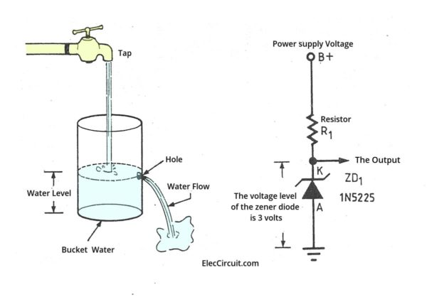
- Faucets compare with power supply.
- Water is like electricity.
- The water level in the can is comparable to Zener voltage. Which will be at the same level as the hole drilled on the side of the can
Here is a step-by-step process.
- When we open the tap. The water will flow from the tap to the can. Which has punctured the side of the can
- When the water level reaches the hole that is drilled, the water will flow out.
- The water level is constant, not likely to be higher than the hole level. So it’s the same as Zener Diode operation.
While supplying the current through R1 to the Zener diode via K, cathode, and pin A, Anode is grounded.
Zener diode part number list
Once we know the desired voltage level, we can select the Zener diode corresponding to or of similar voltage level and the appropriate wattage for our uses.
The higher-wattage Zener diode can be used instead of the lower-wattage one. But the lower one should not be used instead of the higher one. Because in a circuit with a high current, the Zener diode will generate high heat and can be damaged.
I have collected many Zener diodes over the years, but there are many more that I have heard of but never used myself. So, I am going to make a list below of the Zener diodes I have used often.
For example
3 volts ZD (Zener Diode)
If we want a 3V Zener diode, we can use 1N5225 or BZX55C3V0 with the same 3V at 0.5 watts, but if you want higher wattage use 1N4728 (3.3V at 1 watt) instead. This is the Zener diode that provides the closest voltage to 3 volts.
For other numbers:
- BZX79-C3V0 3V 0.4W
- TZX3V0B 3V 0.5W
- 1N4619 3V 0.5W
- TZX3V0C 3V 0.5W
- NZX3V0C 3V 0.5W
- ZPD3.0 3V 0.5W
- 1N4372A 3V 0.5W DO-35
- TZX3V0A 3V 0.5W DO-35
- 1N5987B 3V 0.5W DO-35
- NTE5065A 3V 1W DO-35
- BZX85B3V0 3V 1.3W
5V zener diode number
We can use 5.1V Zener Diode instead. Because we cannot buy 5.0V one. I often use BZX55C5V1, 1N5231B
See the other number below
- BZX79C5V1 5.1V 0.5W
- NZX5V1A 5.1V 0.5W
- TZX5V1B 5.1V 0.5W DO-35
- 1N751A-1 5.1V 0.5W DO-35
- BZX79-B5V1 5.1V 0.4W
- ZPD5B1 5.1V 0.5W DO-35
- 1N4733A 5.1V 1W DO-41
- BZX85C5V1 5.1V 1W
- MAZ20510AG 5.1V 1W DO-41
- BZV85-C5V1 5.1V 1W DO-41
- NTE135A 5.1V 1W
12V ZD (Zener Diode) Number
- 1N5242B 12V 0.5W
- BZX79C12 12V 0.5W
- BZX55B12 12V 0.5W DO-35
- NZX12B 12V 0.5W DO-35
- TZX12D 12V 0.5W DO-35
- NZX12X 12V 0.5W DO-35
- BZX55C12 12V 0.5W DO-35
- 1N759A 12V 0.5W DO-35
- 1N4742A 12V 1W DO-41
- BZV85-C12 12V
- 1N4744A 12V 1W 5%
Other Zener diode parts number list
- BZX55C2V0 (2V)
- BZX55C2V2 (2.2V)
- BZX55C2V4 (2.4V)
- BZX55C2V7 (2.7V)
- BZX55C3V0 (3V)
- BZX55C3V3 (3.3V)
- BZX55C3V6 (3.6V)
- BZX55C3V9 (3.9V)
- BZX55C4V3 (4.3V)
- BZX55C4V7 (4.7V)
- BZX55C5V1 (5.1V)
- BZX55C5V6 (5.6V)
- BZX55C6V2 (6.2V)
- BZX55C6V8 (6.8V)
- BZX55C7V5 (7.5V)
- BZX55C8V2 (8.2V)
- BZX55C9V1 (9.1V)
- BZX55C10 (10V)
- BZX55C11 (11V)
- BZX55C12 (12V)
- BZX55C13 (13V)
- BZX55C15 (15V)
- BZX55C16 (16V)
- BZX55C18 (18V)
- BZX55C20 (20V)
- BZX55C22 (22V)
- BZX55C24 (24V)
- BZX55C27 (27V)
- BZX55C30 (30V)
- BZX55C33 (33V)
- BZX55C36 (36V)
- BZX55C39 (39V)
- BZX55C43 (43V)
- BZX55C47 (47V)
500mW Zener Diode (Nominal Zener Voltage)
- 1N4370A (2.4V)
- 1N4371A (2.7V)
- 1N4372A (3.0V)
- 1N746A (3.3V)
- 1N747A (3.6V)
- 1N748A (3.9V)
- 1N749A (4.3V)
- 1N750A (4.7V)
- 1N751A (5.1V)
- 1N752A (5.6V)
- 1N753A (6.2V)
- 1N754A (6.8V)
- 1N755A (7.5V)
- 1N756A (8.2V)
- 1N757A (9.1V)
- 1N758A (10V)
- 1N759A (12V)
- 1N957B (6.8V)
- 1N958B (7.5V)
- 1N959B (8.2V)
- 1N960B (9.1V)
- 1N961B (10V)
- 1N962B (11V)
- 1N963B (12V)
- 1N964B (13V)
- 1N965B (15V)
- 1N966B (16V)
- 1N967B (18V)
- 1N968B (20V)
- 1N969B (22V)
- 1N970B (24V)
- 1N971B (27V)
- 1N972B (30V)
- 1N973B (33V)
- 1N974B (36V)
- 1N975B (39V)
- 1N5221B (2.4V)
- 1N5222B (2.5V)
- 1N5223B (2.7V)
- 1N5224B (2.8V)
- 1N5225B (3.0V)
- 1N5226B (3.3V)
- 1N5227B (3.6V)
- 1N5228B (3.9V)
- 1N5229B (4.3V)
- 1N5230B (4.7V)
- 1N5231B (5.1V)
- 1N5232B (5.6V)
- 1N5233B (6.0V)
- 1N5234B (6.2V)
- 1N5235B (6.8V)
- 1N5236B (7.5V)
- 1N5237B (8.2V)
- 1N5238B (8.7V)
- 1N5239B (9.1V)
- 1N5240B (10V)
- 1N5241B (11V)
- 1N5242B (12V)
- 1N5243B (13V)
- 1N5244B (14V)
- 1N5245B (15V)
- 1N5246B (16V)
- 1N5247B (17V)
- 1N5248B (18V)
- 1N5249B (19V)
- 1N5250B (20V)
- 1N5251B (22V)
- 1N5252B (24V)
- 1N5253B (25V)
- 1N5254B (27V)
- 1N5255B (28V)
- 1N5256B (30V)
- 1N5257B (33V)
- 1N5258B (36V)
- 1N5259B (39V)
1W Zener Diode (Nominal Zener Voltage)
- 1N4728A (3.3V)
- 1N4729A (3.6V)
- 1N4730A (3.9V)
- 1N4731A (4.3V)
- 1N4732A (4.7V)
- 1N4733A (5.1V)
- 1N4734A (5.6V)
- 1N4735A (6.2V)
- 1N4736A (6.8V)
- 1N4737A (7.5V)
- 1N4738A (8.2V)
- 1N4739A (9.1V)
- 1N4740A (10V)
- 1N4741A (11V)
- 1N4742A (12V)
- 1N4743A (13V)
- 1N4744A (15V)
- 1N4745A (16V)
- 1N4746A (18V)
- 1N4747A (20V)
- 1N4748A (22V)
- 1N4749A (24V)
- 1N4750A (27V)
- 1N4751A (30V)
- 1N4752A (33V)
- 1N4753A (36V)
- 1N4754A (39V)
- 1N4755A (43V)
- 1N4756A (47V)
- 1N4757A (51V)
- 1N4758A (56V)
- 1N4759A (62V)
- 1N4760A (68V)
- 1N4761A (75V)
- 1N4762A (82V)
- 1N4763A (91V)
- 1N4764A (100V)
3.5W Zener Diode (Nominal Zener Voltage)
- 1N1588 3.9V 10 %
- 1N1588A 3.9V 5 %
- 1N1589 4.7V 10 %
- 1N1589A 4.7V 5 %
- 1N1590 5.6V 10 %
- 1N1590A 5.6V 5 %
- 1N1591 6.8V 10 %
- 1N1591A 6.8V 5%
- 1N1592 8.2V 10 %
- 1N1592A 8.2V 5 %
- 1N1593 10V 10 %
- 1N1593A 10V 5 %
- 1N1594 12V 10 %
- 1N1594A 12V 5 %
- 1N1595 15V 10 %
- 1N1595A 15V 5%
- 1N1596 18V 10 %
- 1N1596A 18V 5 %
- 1N1597 22V 10 %
- 1N1597A 22V 5 %
- 1N1598 27V 10 %
5W Zener Diode (Nominal Zener Voltage)
- 1N5333 3.3V
- 1N5334 3.6V
- 1N5335 3.9V
- 1N5336 4.3V
- 1N5337 4.7V
- 1N5338 5.1V
- 1N5339 5.6V
- 1N5340 6.0V
- 1N5341 6.2V
- 1N5342 6.8V
- 1N5343 7.5V
- 1N5344 8.2V
- 1N5345 8.7V
- 1N5346 9.1V
Basic Zener diode forward bias and the reverse bias
The Zener diode always keeps the voltage drop across it at 3V. The remaining voltage will drop across the resistor.
Not only that, See the next circuit diagrams.

See an example of the basic Zener diode between a forward bias (A) and the reverse bias (B).
- Look at the circuit A. When we enter a forward bias voltage. (At the anode pin has more voltage than the cathode). The positive current enters the anode of Zener Diode (ZD1) via Resistor (R1). The operation of a Zener diode is like a general diode. It will allow the current to flow through it. And there is the voltage drop across about 0.6V. The rest of the voltage is across the resistor. When the voltage of the Zener diode is combined with the resistor, We get the voltage equal to the power supply.
- Look at the circuit B. In contrast, when we enter a reverse bias (The cathode pin has more voltage than the anode pin) to a Zener diode. This time, the Zener Diode will have different features than normal diodes. The common diodes will not allow currents to flow through them. But in this, the Zener diode will allow the current to pass through it. Only when the voltage across the bias reverse is greater than the Zener diode voltage. In this, it works. Because the power supply is 6V. And the voltage of the Zener diode is 3V. And, the voltage across the Zener diode is constant. It is the breakdown voltage level as above.
We can change this voltage level(Vz). By changing the number of Zener diode, which the manufacturer has specified, there are many numbers and many sizes as mentioned above.
What is more? We will learn them with many example circuits below.
How to use Zener diode
Normally, Zener diode is used as the regulator circuit. There are many forms, as follows.
Simple current and constant voltage regulator
Look at the basic circuit below. It is low current regulator circuit. Which is determined by the resistor R1. And the output voltage has a constant value equal to the zener diode voltage in any loads.
We can calculate the appropriate resistance of R1 using the formula:
R1 = (Vin – Vz)/(IL + Iz)
Most in practice. The current-Iz, while the load connected. We usually set it to 5mA. So we get a new formula.
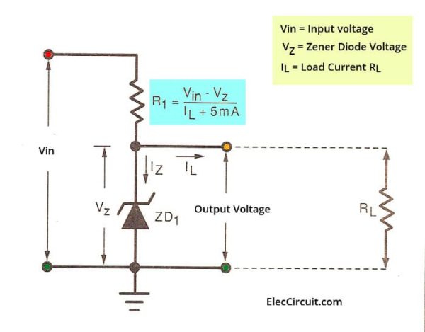
R1 = (Vin -Vz)/(IL + 5mA)
So, Choosing the resistance to depend only on the current flowing through the load. But if wanting to calculate for use in real work.
We have to offset for IZ current. While there is no load as well.
Because while there is no continue loading The current will flow through all Zener Diodes. It should allow for the wattage of Zener Diode to endure while no-load as well.
Want to see real calculate to find R1?
Read Also: 5V Zener regulator low current
Choosing a Zener Diode. We need to look at the watts that the Zener diode can tolerate. Which is calculated as follows: The wattage power lost in the Zener Diode (P) is equal to the Zener diode voltage (Vz) times the current passing through the Zener diode (Iz).
P = Vz x Iz
Note: Iz is obtained from the voltage across the resistor divided by the resistance of that resistor(R).
Do you get an idea?
Basic Higher current Zener and transistor regulator
Look at the circuit below. It is similar to the previous circuit. But it can supply a higher current. Because the transistor is a helper to increase current up.

We connect it in serial before output. Then use a Zener diode voltage as a bias voltage for the Transistor. The output voltage of this circuit is less than Zener diode about 0.6V.
Because the voltage of Zener Diode will drop across between base and emitter of transistor about 0.6 volts.
The maximum current that the circuit can supply depends on the capability of the transistor.
If the transistor highly withstands to current. It can supply a lot of currents. And, on the other hand, if there is little resistance. it will supply lower current.
Parts lists
- Q1: 2N3053, 0.7A 40V NPN Transistor
- ZD1: 12V 0.5W Zener Diode
- C1: 10uF 16V Electrolytic Capacitor
- R1: 1.2K 0.25W 5% Resistor
- R2: 4.7K 0.25W 5% Resistor
Check out these related circuits, too:
- 100mA 5V converter circuit
- Small Zener diode voltage regulator circuit with PCB
- 9V regulated power supply circuit
Do you observe? The output is 11.4V only but we want 12V. How do you do?
Then, The solution to the problem is to make the output voltage equal to the Zener diode voltage.
Look at the circuit diagram. Add Diode to offset B-E transistor voltage.

By bringing the Rectifier Diode to a series with a Zener diode. Because of the voltage across the diode, it will just offset the voltage across the pin B-E of the transistor.
The output voltage is therefore equal to the Zener Diode voltage.
Make 3V DC regulator using Zener Diode and transistor
Is it easier? If we use suitable Zener.
Look at the true circuit.

We use the Zener Diode No. 1N5227 or BZX55C3V6. It has a Zener Diode voltage equal to 3.6V.
When the current flows through the base to emitter. There will be the voltage across the base and emitter about 0.6V.
Therefore need to reserve another 0.6V. The output voltage is approximate 3V
For other devices, it has the same principle of DC power supply.
When the transformer reduces the voltage to 9V, it will pass the rectifier diodes D1 and D2 (full-wave rectifier) to be DC voltage.
Then C1 will make the DC current smoother. It passes Resistor R1 to the cathode of Zener Diode.
Next, C2 is a filter capacitor to keep stable Zener voltage. And C3 also is a filter capacitor to reduce a ripple.
This circuit can give output 3V at 800mA max.
See parts list below
- Q1: 2SC1061, 4A 40V NPN transistor
- ZD1: 3.6V 0.5W Zener diode ,1N5227 or BZX55C3V6
- D1,D2: 1N4001, 1A 50V Diode
- R1: 5K 0.25W 5% Resistor
- C1,C3: 1,000uF 16V Electrolytic Capacitors
- C2: 1uF 16V Electrolytic Capacitor
- T1: 117V/230V AC primary to 9V-0-9V,1A secondary transformer
Voltage comparator Zener op-amp regulator
What is a better circuit?
In addition to this method, we also have a way to compare the output voltage with the Zener diode voltage. By using an op-amp as a comparator. As Figure below.

When the power goes into the input, there is a voltage across the 12V Zener diode. Therefore, pin 3 of the op-amp (CA3140) has the voltage is equal to 12V as well.
When the power goes into the input, there is a voltage across the 12V Zener diode. Therefore, pin 3 of op-amp has the voltage is equal to 12V, too.
It causes the output-pin 6 of an op-amp is a positive voltage. To bias Q1 works. So, there is the current flows through pins C-E and R3.
If pin 2 and pin 3 are higher then the voltage will come out pin 6. To bias Q1, has more current flows. Until the voltage pin 2 and 3 are equal.
We will see this circuit has high stability than only one transistor.
Parts you will need
- IC1: CA3140, 4.5MHz, Bimos Operational Amplifier With MOSFET Input/Bipolar Output
- ZD1: 12V 0.5W Zener diode
- C1: 10uF 25V Electrolytic capacitor 0.25W Resistors, tolerance: 5%
- R1, R3: 1.2K
We can see that the Zener Diode is used in various circuits.
Here are a few related posts you might want to read:
- Super Steady Zener diode voltage regulator circuit
- Variable zener diode circuit, adjust voltage output
- Power Supply for Audio Amplifier , multiple output 12V, 15V, 35V
GET UPDATE VIA EMAIL
I always try to make Electronics Learning Easy .
Related Posts
I love electronics. I have been learning about them through creating simple electronic circuits or small projects. And now I am also having my children do the same. Nevertheless, I hope you found the experiences we shared on this site useful and fulfilling.
9 thoughts on “What is Zener diode? Its principle working and example usage”
I am 72 years old but I always like electronics I don’t know that much but I find it interesting. Regards Roger.
Thanks so much for your feedback.
It makes me so happy.
Did you know that You are the same age as my father?
I promise to make electronics easy for you. I hope my dad likes electronics like you. Because it could help reduce his memory loss. You probably have a good memory, right?
Thanks again. Apichet
Good to be among professionals
Hi katongo, Thanks for your feedback.
Can you explain to me why Basic Higher current Zener and transistor regulator if you should not look at resistor R1 but in transistor to give higher current. Somewhere I have read that resistor R1 is essential to give higher current to a circuit.
Hello Tomasz, It is glad that you are interested in the power supply. I love it. Yes, In the power supply. We use a Zener diode and transistor often.
A resistor affects the current of the load as well. It passes the current to a Zener diode and most current to the load.
Then, we add a transistor. Also, a resistor is a device that passes a bias current for the transistor to operate. The more current flows through the transistor to the load.
In the past, I didn’t really understand how this works. But when trying to build these circuits, and compare them so more understandable
PS. I am not quite sure. I will clearly understand your question. My English is quite poor.
The water tank zener analogy is not really demonstrative of a zener. A better 1st order anology would be a mechanical spiral tension spring with loops at each end. Then with a bolt through it and a nut setting the max elongation of the spring(to mimic Vzener). Then some mechanism to not allow a reverse elongation as the zener will act as a regular diode if reversed.
Hi, Thank you very much for your advice. I’m currently studying about Zener diodes. Your suggestions are very helpful to me. And I will learn more.But I am a slow learner and not very good at it. 🙂
The water tank analogy as given is incorrect. The pressure (voltage) on the output is effectively zero unless the tap is so wide open that the water backs up in the can.
A can with a wide overflow at the top so that most of the water flows out will give a fixed pressure (voltage) at an outlet at the bottom of the can, but this analogy also fails because there is no excess current outlet in a Zener Diode.
Leave a Comment Cancel reply
Save my name, email, and website in this browser for the next time I comment.
This site uses Akismet to reduce spam. Learn how your comment data is processed .
- My Workbench
- Electronics Q&A
Zener diode voltage reference PUBLIC
| Created by | |
| Created | November 13, 2011 |
| Last modified | June 08, 2017 |
| Tags |
A Zener diode provides controlled reverse breakdown, and can act as a fixed voltage reference.
Link & Share
Copy and paste the appropriate tags to share.
Schematic PNGs: (download or hot-link) small , medium , large
CircuitLab forums and comments:
BBCode (many online discussion forums):
- Export SVGZ
Description
Zener diode D1 provides a fixed breakdown voltage of about 5.1 volts over a wide range of currents. R1 is necessary to prevent over-loading of voltage source V1.
Using a Zener diode like this isn't a particularly efficient way to generate a fixed voltage reference due to the high currents involved, but it's quite simple and reliable.
A few things to try in CircuitLab
This circuit highlights several cool features of CircuitLab simulations that you can quickly try. Load this circuit with the "Open in editor" button above, and then click the "Simulate" tab to get started.
You can see the output voltage (near 5.1V) as well as the DC current running through the Zener diode -- those things can get quite hot!
Use the DC sweep to simulate how the output voltage will be affected if the input voltage changes. As you can see, the output remains quite close to 5.1V over many volts of input voltage.
You can plot the frequency response of this voltage reference, which might be useful if you have a noisy power supply (V1), and are curious to know how much of that noise makes it into the "regulated" voltage V(out). As you can see, with the current parameters, there's about -40dB gain between V(in) and V(out). This means that a ripple at the input will cause a ripple about 1/100th as big at the output -- not a bad start for power supply noise rejection.
| how can current pass through the anode of zener? the direction is from cathode to anode | by |
| Try it! You will be impressed. A Zener in the reverse voltage mode will break down at the Vz value and start to conduct. Its current can vary but the voltage that is dropped across the zener will remain fairly constant at the Vz value. About 5% (not real good conpaired for todays advanced circuits) but as the auoher said, " this circuit works well and is very stable." That's how the zener works. | by |
| Why is there a current source on this circuit? | by |
| The current source is used as a load. With this arrangement the voltage on the output can vary with the Vz while maintaining a constant current. In this case a load of 10 ma. If your circuit is not pulling a constant load then remove the current source. | by |
Leave a Comment
Please sign in or create an account to comment.
Revision History
Only the circuit's creator can access stored revision history.
- Zener Diode As A Voltage Regulator
Zener Diode as a Voltage Regulator
Zener diode is a silicon semiconductor with a p-n junction that is specifically designed to work in the reverse biased condition. When forward biased, it behaves like a normal signal diode, but when the reverse voltage is applied to it, the voltage remains constant for a wide range of currents. Due to this feature, it is used as a voltage regulator in d.c. circuit. The primary objective of the Zener diode as a voltage regulator is to maintain a constant voltage. Let us say if Zener voltage of 5 V is used then, the voltage becomes constant at 5 V, and it does not change.
What is a Voltage Regulator?

- To vary or regulate the output voltage
- To keep the output voltage constant at the desired value in spite of variations in the supply voltage.
Voltage regulators are used in computers, power generators, alternators to control the output of the plant.
There is a series resistor connected to the circuit in order to limit the current into the diode. It is connected to the positive terminal of the d.c. It works in such a way the reverse-biased can also work in breakdown conditions. We do not use ordinary junction diode because the low power rating diode can get damaged when we apply reverse bias above its breakdown voltage. When the minimum input voltage and the maximum load current is applied, the Zener diode current should always be minimum.
Since the input voltage and the required output voltage is known, it is easier to choose a Zener diode with a voltage approximately equal to the load voltage, i.e. VZ = VL .
Following is the link explaining the difference between Zener breakdown and Avalanche breakdown:
The circuit diagram of a voltage regulator using a Zener diode is shown:

Current through the diode increases when the voltage across the diode tends to increase which results in the voltage drop across the resistor. Similarly, the current through the diode decreases when the voltage across the diode tends to decrease. Here, the voltage drop across the resistor is very less, and the output voltage results normally.
Read more to learn about the Zener diode as a voltage regulator, uses of a Zener diode , and how it is used as a voltage regulator with BYJU’S engaging videos.
Frequently Asked Questions – FAQs
Name the factor which is required for voltage regulation to keep diode in the breakdown region..
Minimum reverse current is required for voltage regulation to keep the diode in the breakdown region.
How to set the breakdown region during manufacturing of the diode?
By controlling the doping level, the breakdown region can be set during the manufacturing of the diode.
What is a Zener breakdown?
When the breakdown occurs in Rectifier as well as the Zener diode, it is known as the Zener breakdown.
What happens to the DC output voltage when the input varies within the limits?
The DC output voltage remains constant when the input varies within the limits as the voltage regulator is used.
State true or false: Voltage regulator is used to vary or regulate the output voltage.

Put your understanding of this concept to test by answering a few MCQs. Click ‘Start Quiz’ to begin!
Select the correct answer and click on the “Finish” button Check your score and answers at the end of the quiz
Visit BYJU’S for all Physics related queries and study materials
Your result is as below
Request OTP on Voice Call
| PHYSICS Related Links | |
Leave a Comment Cancel reply
Your Mobile number and Email id will not be published. Required fields are marked *
Post My Comment
Register with BYJU'S & Download Free PDFs
Register with byju's & watch live videos.

What is a Zener Diode? How Does it Work? Where to Use? ( Zener Diode Tutorial)

一款好用到爆的AI搜索工具!
COMMENTS
Zener Diode Explanation. A Zener Diode, also referred to as a breakdown diode, is a specially doped semiconductor device engineered to function in the reverse direction. When the voltage across a Zener diode's terminals is reversed and reaches the Zener Voltage (also known as the knee voltage), the junction experiences a breakdown, allowing ...
This resource contains information on diodes, ideal diode model, full diode model, offset voltage model, half wave rectifier, full awve rectifier, and zener diode. 17_diodes1.pdf | Introduction to Electronics, Signals, and Measurement | Electrical Engineering and Computer Science | MIT OpenCourseWare
A Zener diode is a type of diode that is often used for voltage regulators and shaping waveforms. Its symbol is an arrow pointing towards a crooked line. There are actually three different ways you can draw the Zener diode symbol in schematics: Three ways to draw the Zener Diode Symbol. While a normal diode only allows current to flow through a ...
2/27/2012 section_3_4_Zener_Diodes 1/3 Jim Stiles The Univ. of Kansas Dept. of EECS 4.4 Operation in the Reverse Breakdown Region — Zener Diodes Reading Assignment: pp. 190-191 A Zener Diode is simply a p-n junction diode that is meant to be operated in breakdown. Understanding the differences between a Zener diode and a junction diode is ...
A Zener diode is a special type of diode designed to reliably allow current to flow "backwards" (inverted polarity) when a certain set reverse voltage, known as the Zener voltage, is reached.. Zener diodes are manufactured with a great variety of Zener voltages and some are even variable. Some Zener diodes have an abrupt, heavily doped p-n junction with a low Zener voltage, in which case the ...
Since a zener diode is designed to work in the reverse breakdown region of its characteristic curve, they have a fixed breakdown voltage, V Z value which is determined during manufacture. As the reverse voltage across the zener diode increases from 0 volts to its zener breakdown voltage, a small reverse or leakage current will flow through the diode which remains fairly constant as the reverse ...
Breakdown Region — Zener Diodes Reading Assignment: pp. 167-171 A Zener Diode Æ A junction diode that is meant to be operated in breakdown. The 3 technical differences between a junction diode and a Zener diode: 1. 2. 3. The practical difference between a Zener diode and "normal" junction diodes: Î Manufacturer assumes diode will be ...
Zener diode clipper: The Zener breakdown voltage for the diodes is set at 10 V by the diode model parameter "bv=10" in the spice net list in Figure above. This causes the Zeners to clip at about 10 V. The back-to-back diodes clip both peaks. For a positive half-cycle, the top Zener is reverse biased, breaking down at the Zener voltage of 10 V.
A Zener diode operating in breakdown acts as a voltage regulator because it maintains a nearly constant voltage, which is equal to the Zener voltage, across its terminals over a specified range of reverse-current values. This constant voltage drop across the Zener diode produced by reverse breakdown is represented by a DC voltage symbol.
A Zener diode is a type of PN junction diode that is designed to conduct in both forward and reverse directions. It has heavily doped regions and is mainly used to conduct current in the reverse direction. It starts conducting in the reverse direction when the reverse voltage exceeds a certain limit known as the reverse breakdown or Zener ...
Zener Diode PDF Link - https://bit.ly/3iI7vLH Physics Formulae Revision Playlist - https://bit.ly/3eBbib9 JULY Attempt Solution JEE Main 2021 PLAYLIST - htt...
Zener Diode is one of the most important semiconductor diodes used in our daily life. It is a specific diode that works in reverse bias conditions. It allows current to flow from anode to cathode and it also works in the reverse direction. Let's learn about Zener Diodes their function, and their construction, in detail in this article.
A Zener diode is a diode which allows current to flow in the forward direction in the same manner as an ideal diode, but will also permit it to flow in the reverse direction when the voltage is above a certain value known as the breakdown voltage ... Assignments. 1. Study the variation of current flowing through the zener diode for different ...
Assignment References Theory Objective. At the end of the experiment, the student will be able to Explain the function of a Zener diode; Explain Zener Diode as Voltage Regulator; Zener Diode. A Zener Diode is a special kind of diode which permits current to flow in the forward direction as normal, but will also allow it to flow in the reverse ...
A Zener diode is a semiconductor device that makes the current flow in the forward or in the backward direction. The diode usually consists of a p-n junction which is heavily doped. The diode is designed to conduct the flow of current in the reverse direction after reaching a specified voltage. The Zener diode has a reverse-breakdown voltage at ...
In this lab, students will focus on Zener diodes, including their theory of operation, applications, and uses. They will first observe the function of a zener diode when used as a voltage regulator in circuit simulation. Then they will implement and test the circuits using the NI ELVIS III breadboard and IV Analyzer by appling voltage to a load through a zener diode.
The forward bias region of a Zener diode is identical to that of a regular diode. The typical forward voltage at room temperature with a current of around 1 mA is around 0.6 volts. In the reverse bias condition the Zener diode is an open circuit and only a small leakage current is flowing as shown on the exaggerated plot.
The operation of a Zener diode is like a general diode. It will allow the current to flow through it. And there is the voltage drop across about 0.6V. The rest of the voltage is across the resistor. When the voltage of the Zener diode is combined with the resistor, We get the voltage equal to the power supply.
Description. Zener diode D1 provides a fixed breakdown voltage of about 5.1 volts over a wide range of currents. R1 is necessary to prevent over-loading of voltage source V1. Using a Zener diode like this isn't a particularly efficient way to generate a fixed voltage reference due to the high currents involved, but it's quite simple and reliable.
Zener diode is a silicon semiconductor with a p-n junction that is specifically designed to work in the reverse biased condition. When forward biased, it behaves like a normal signal diode, but when the reverse voltage is applied to it, the voltage remains constant for a wide range of currents. Due to this feature, it is used as a voltage ...
Zener diode is a diode that keeps the voltage applied to its pins constant. When zener diodes are connected to the circuit in the right direction, it works like a normal silicon diode. In other words, they start to flow current after 0.7V. But they are not used that way. They are used in reverse connection to the circuit.